By Nasheed Ur Rehman, Head of Forward Deployed Engineering
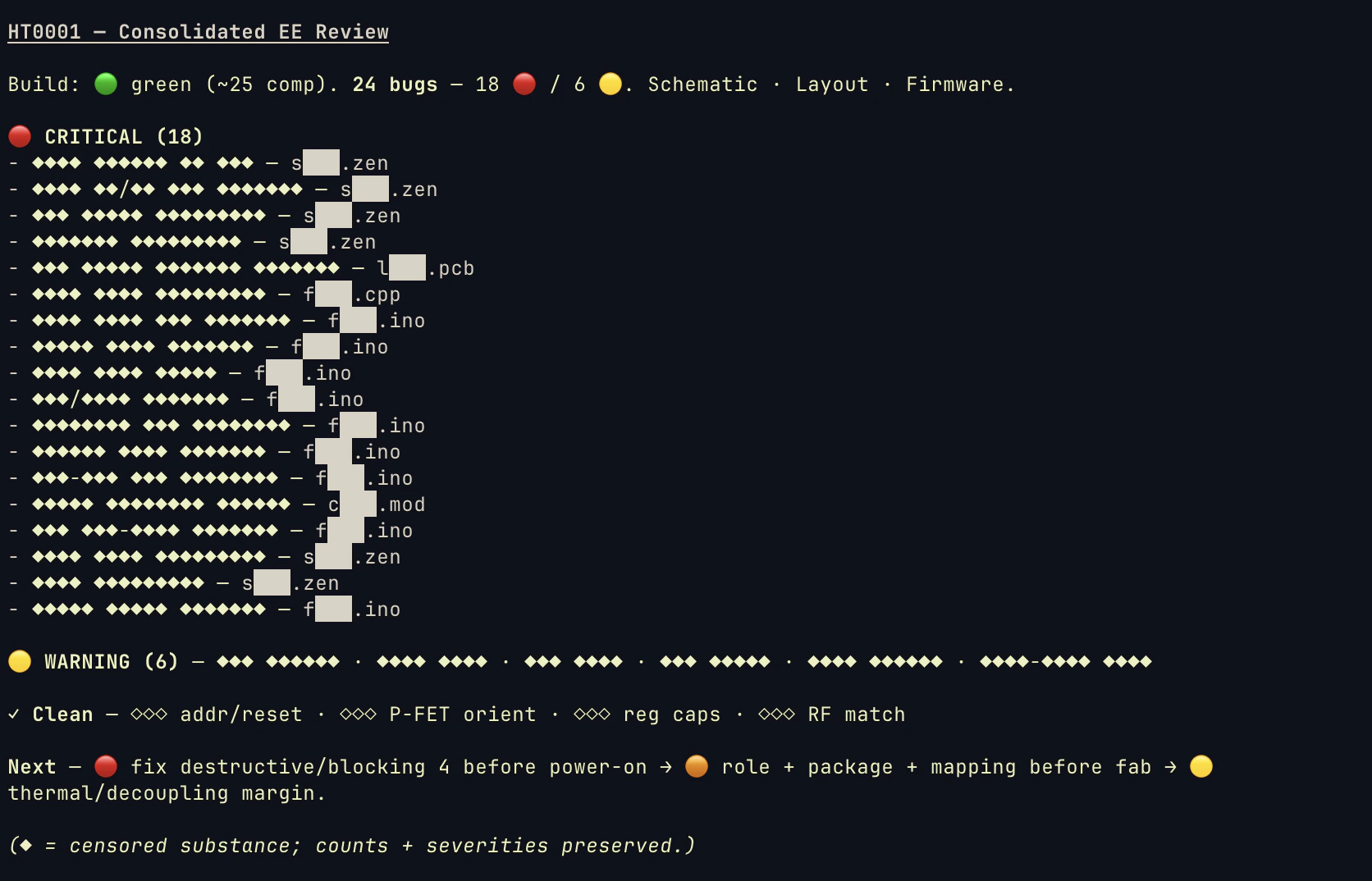
Last week, comma.ai reposted its hardware challenge. It is a good challenge. The premise is simple: they designed a wire harness tester, added bugs to the schematic, layout, and firmware, and asked people to find what was wrong. Our CTO, Lenny Khazan, decided to throw Diode’s internal tooling at it. The challenge ships as a KiCad project, so the first step was importing it into Zener — our open-source language for describing PCBs as code — to give the reviewer the structured representation it needs. With a few prompts, the tool found 22 bugs and won the $1000 prize.
The interesting part is not the prize. The interesting part is what had to exist for that to be possible. I remember trying the comma challenge when I was in college. It was fun in the way hard things are fun. You start by opening the schematic and thinking you will find a few obvious issues. Then, very quickly, you are deep in the work. You are probing individual nets. You are opening datasheets. You are checking whether a pin is actually the pin you think it is. You are comparing connector mappings, regulator topologies, protection circuits, and interface requirements. After a few hours, you realize something slightly unsettling: you are not really “checking a board.” You are reconstructing the intent of the engineer who designed it. That is what makes PCB review hard.

How a board can fail

A PCB can fail in a few broad ways. The first class is design failure. The schematic is wrong. A pin is floating. A regulator feedback network is incorrect. A reset pin is not pulled to the right state. A part is being used outside its recommended operating conditions. The second class is implementation failure. The schematic may be mostly right, but the layout is wrong. The decoupling capacitor is too far from the pin it is supposed to support. A high-speed signal loses its reference plane. A current path necks down somewhere inconvenient. Differential pairs are routed as if they are decorative. The third class is manufacturing and assembly failure, which is its own universe of problems: wrong parts, wrong packages, bad solder joints, tombstoning, polarity mistakes, and all the ways a thing that was correct in CAD can still become wrong in the real world. Most tools only cover a slice of this. DRC tells you whether your layout violates a set of geometric rules. ERC tells you whether some obvious electrical relationships look suspicious. BOM tools can tell you whether a part exists, maybe whether it is expensive, maybe whether it is out of stock. These are all useful. But none of them really answer the question an experienced EE is asking during a review: “Is this actually going to work?”

Intent lives outside the file

That question is hard because the answer depends on intent. A schematic is not just a graph of nets. It is a compressed explanation of what the board is supposed to do. Some of that explanation is explicit: net names, page titles, component choices, annotations. But a lot of it lives outside the file. It lives in the datasheet the engineer read three weeks ago. It lives in the reference design they copied but modified. It lives in the assumption that this enable pin will be driven later, or that this connector pinout matches a cable, or that this ADC input will never exceed a certain voltage. When you review someone else’s board, you have to recover all of that context. This is why the comma challenge is interesting. It is not merely a puzzle. It is a compact version of a real engineering problem: can you inspect a hardware design deeply enough to find the bugs that matter before the board is built?

What we are building at Diode

Consolidated EE Review of the comma harness tester: 24 bugs surfaced — 18 critical, 6 warnings — across schematic, layout, and firmware Reviewer output on the comma harness challenge — bug descriptions censored to keep the puzzle intact for future challengers, but the counts and severities are real. At Diode, we have been building an AI electrical engineering reviewer for exactly this kind of work. It is not a chatbot that says generic things about decoupling. It is a design reviewer that reads real hardware projects: schematics, PCB layouts, Zener modules, KiCad projects, and BOMs. It is read-only. It does not edit your files. It investigates and reports findings. The reviewer looks for the same classes of problems a careful electrical engineer looks for. It checks schematic correctness: floating pins, missing pull-ups, bad enables, shorted nets, incorrect connector pinouts, missing feedback components, and logic-level mismatches. It checks datasheet compliance: recommended application circuits, decoupling requirements, absolute maximum ratings, operating conditions, power sequencing, and interface requirements. It checks power integrity and protection: regulator stability, capacitor selection, current limits, reverse polarity protection, ESD, surge paths, grounding, and return currents. When layout files exist, it inspects physical implementation: decoupling placement, high-current trace width, return paths, sensitive routing, crystal placement, clearances, thermal copper, and vias. It can also inspect BOMs for invalid part numbers, value mismatches, package mismatches, derating issues, and sourcing risk. The important part is that it does not try to sound smart. It tries to be useful. That means it should not invent findings. If there is no evidence, there is no report. Findings are prioritized by severity: critical issues that can make the board nonfunctional or damaging, warnings that are likely problems or datasheet deviations, and notes that are worth verifying. This is a subtle but important distinction. A bad AI reviewer is worse than no reviewer, because it creates work. It fills the review with plausible nonsense, and now an engineer has to review the review. The goal is not to produce a long report. The goal is to find the small number of things that would actually make you regret ordering the board.

Why this works: Zener

The reason this works at Diode is Zener. Zener is our open-source language for describing PCBs as code. A board written in Zener is not just a drawing. It is a structured representation of components, nets, interfaces, modules, and constraints. It can render into normal schematics for humans, but underneath it has the properties software engineers expect: it is readable, composable, version controlled, reviewable, and testable. This matters because models are much better when the thing they are reasoning about has structure. Traditional EDA tools were built for humans looking at drawings. That is still important. Engineers should be able to inspect a schematic visually. But models need a different interface. They need to trace relationships, jump between modules, inspect symbols, compare intent to implementation, and connect datasheet requirements to actual nets and components. Zener gives the model something closer to source code. It turns hardware into a workflow where a model can reason about the design instead of just staring at screenshots of it.

Review is many tasks stacked together

The comma challenge is a clean demonstration of this broader point. Hardware review is not one task. It is many tasks stacked together. You have to understand what the board is supposed to do. You have to identify the critical components. You have to read the datasheets. You have to know which recommendations are optional and which are not. You have to trace the schematic. You have to inspect the layout. You have to notice when a part is electrically correct but physically implemented in a way that defeats the point. You have to decide whether something is a real bug or merely a design choice you would not have made. That is precisely the kind of work AI can help with, if the workflow is built correctly. Not by replacing the engineer. By giving the engineer a tireless second reviewer. A good reviewer does not get bored halfway through a 90-page datasheet. It does not forget to check the enable pin because the power tree looked fine. It does not skip the layout because ERC passed. It can follow a net through the project, look up the device requirements, compare them against the schematic, then ask whether the layout preserves the assumptions the schematic made. It is still not magic. It cannot guarantee production readiness. It does not replace lab validation, EMC testing, SI/PI, thermal testing, certification, or final sign-off. Firmware and bring-up can be increasingly automated, but real hardware still needs to be measured and validated. It can be wrong. It can miss things. But so can people. The right comparison is not AI versus a perfect engineer. The right comparison is AI plus an engineer versus the process most boards actually get: one tired person reviewing a design under schedule pressure, with some checks automated and many assumptions left implicit.

Closing the gap

PCB review has always had a tooling gap. We have excellent tools for drawing boards. We have manufacturing checks. We have simulation for certain domains. But the everyday act of asking “is this design electrically sane?” is still surprisingly manual. That is the gap we are trying to close. The future of PCB design will look more like software. Designs will live in structured representations. Reviews will be diffable. Reference circuits will be reusable. Constraints will travel with modules. Models will inspect boards continuously, not just at the end. Engineers will spend less time hunting for missing pull-ups and more time deciding what the system should be. The comma challenge was designed as a hiring screen. It asks a useful question: Can you find the bugs? Increasingly, the better question may be: can your tools help you find them before they become hardware? Because the cost of a missed bug is not a lower leaderboard score. It is a board spin.